The Dream Material, Carving Semiconductors into Glass.
Advanced TGV Glass Substrate Solutions Powered by Ultra-Precision Processing
Glass substrates are semiconductor bases made from glass, replacing conventional plastic materials. Applying glass instead of plastic allows for:
· Thinner semiconductor packages
· Up to 50% reduction in power consumption
· Significant improvement in data processing capabilities
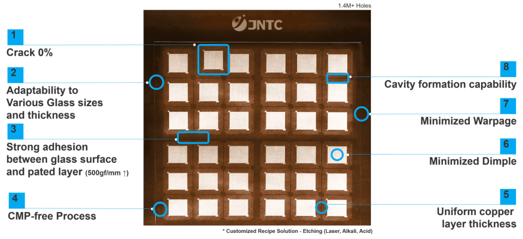
JNTC possesses advanced technologies essential for glass-based semiconductor packaging, including:
· Glass cutting for substrate processing
· Laser Through Glass Via (TGV) formation
· Electrode plating for glass packaging substrates










 EN
EN